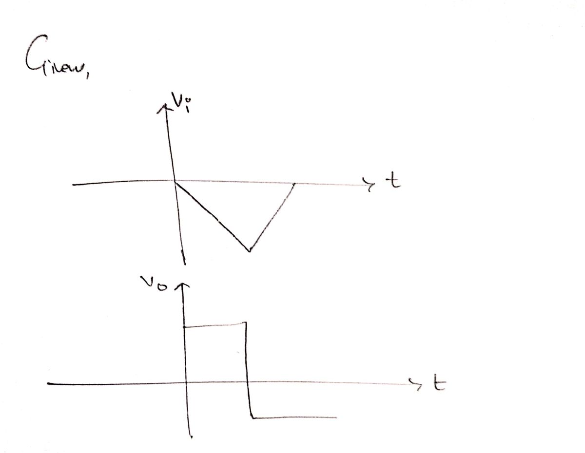
Which circuit would cause this output signal given this input signal? Input signal Vi Output signal Vo


Q: Explain and if possible with graph. What happens to the oscillation when R4 is varied to a larger…
A: According to the question, we need to explain the effect on oscillation if R4 is varied to a larger…
Q: (b) Another of the blocks in the diagram is labelled sample-and hold. (i) Explain the purpose and…
A: (i) to explain the operation and principle of the sample and hold circuit (ii) the sample period is…
Q: design monostable multivibrator,astable mutivibbrator, bistable multivibrator using multisim by…
A: A multi-vibrator is an electronic circuit used to implement a variety of simple two-state devices…
Q: Choosing a discrete value that is near but not exactly at the analog signal level leads to Select…
A: Quantization error is the difference between the analog signal and the closest available digital…
Q: What is the output when the input voltageisless than, greater than, andequaltothe refence voltage?
A: Assuming the given device to be an OPAMP comparator i.e.,
Q: The given Oscillator, a) Draw the small sign model, b) Determine the oscillator frequency and…
A:
Q: Find the value of Rf necessary to produce an output that is 10 times the sum of the inputs in the…
A:
Q: 18. Determine the decimal output value för the se 4. 6 7. 1 CLK MSB=Q2 Q1 LSB Q0
A: Steps: Find the each Output bit value from the diagram Check MSB,intermediate bit and LSB Arrange…
Q: Explain and if possible with graph. What happens to the oscillation when R4 is varied to a larger…
A: The circuit diagram of wein bridge oscillator is shown below,
Q: An amplifier with automatic gain control (AGC) has less gain when the input voltages is high than…
A: Automatic Gain Control (AGC) amplifiers are another category of amplifiers whose gain can vary…
Q: small signal amplifier as shown in the picture. If the input signal is sinusoidal 1 mVpp and β =…
A:
Q: Q\ In an Encoder circult when n=7 and for inPut scale of oolooou, the ouput Valueiso e b) oto
A: This problem comes under digital electronics . It is based on the working of encoder . Encoder is a…
Q: How can the amplitude of the output voltage be increased?
A: This question is related to analog circuits. The amplitude of the output voltage can be increased…
Q: Calculate the input impedance for small-signal equivalent circuit
A: Calculate the input impedance for small-signal equivalent circuit ?
Q: Obtain the waveform of output states Q and ̅for the SR when the input condition as in figure 5 is…
A:
Q: Obtain the waveform of output states Q and ̅for the SR when the input condition as in figure 5 is…
A: Note: In the question it given SR but in figure it is given JK flip flops so assuming the JK for…
Q: The signal level at the input of the amplifier is 120 mV, and the hoise level is 6mV. Calculate the…
A:
Q: Consider the circuit below, assume that the input offset voltage is at its maximum value
A: Operational amplifier- An integrated circuit which amplifies weak electric signals into a strong…
Q: Draw schematic diagram of summing amplifier
A: Summing amplifier is used to convert multiple input voltage at input terminal into single output…
Q: How does the voltage gain compared to the power gain.
A: We are authorized to answer one question at a time, since you have not mentioned which question you…
Q: Consider the analog signal
A: We are authorized to answer three subparts at a time, since you have not mentioned which part you…
Q: 1- Discuss active high whens and R are one
A: According to guidelines we need to solve only the first question. According to the question we have…
Q: b) Considering the average input voltage found in (a), what will be the minimum value of R₂?
A: Given data, The maximum Zener current (Izmax)=100mA The maximum Zener Power dissipation (Pz)=1W The…
Q: Find stability of the system -alti h Ct) = e
A: If integration yields a finite values then the system is said to be stable
Q: Draw the small signal equivalent circuit. Determine the following: Zo Zin Av (voltage gain) Ai…
A: The required parameters can be calculated by using the DC and AC analysis of the cascade amplifier.
Q: "DO Vosto M2 Jout mi Vin show small signal model and find the voltage gain
A: Brief description: Generally in case of MOSFET transistors the current flowing into the gate…
Q: 6) Consider the following multistage amplifier. Draw the corresponding small signal model. Label,…
A: The small signal equivalent circuit can be obtained by replacing the transistor with its equivalent…
Q: Rf Rf Vin Ri TL074 Vout Ri TL074 Vout + Ro Ro Vin Figure A: Inverting Amplifier Figure B:…
A:
Q: true or false A voltage buffer circuit provides a means of matching between input signal and a load…
A:
Q: Another of the blocks in the diagram is labelled sample-and hold. (i) Explain the purpose and…
A: All the physical signal are analog in nature. To process such a signal using a DSP (Digital Signal…
Q: What is the minimum input voltage required for regulation that should be established in the circuit…
A:
Q: Clamper circuit: Vi (p-p)= 10 volt (Sinewave) F=1 kHz R= 10 Kohm V= 4 volt C= 1 micro F Find and…
A:
Q: Given Vi = 20V peak-to-peak, draw the output waveform for the said clamper circuit below:
A:
Q: For the circuit shown in the adjacent figure: a) What type of biasing shown in figure? b) Determine…
A: The given biasing is collector feedback biasing.
Q: The DC power to a modulated class C amplifier is 500 Watts. Determine the power the modulator must…
A: From the question, it is given that Pc=500 W, m=1
Q: u pornt Radix-2 DIF F Fl HiW2; Drow The signal flow graph for HiWili Draw The signal flow graph forr…
A: 1) The signal-flow graph for 4-point Radix-2 DIF FFT: where is twiddle factor.
Q: Find the voltage gain of the OP-AMP.
A: To answer above question, one should know what an amplifier is. An amplifier is an electronic…
Q: What is the word that signals you to add two on the active number of coils to get the actual number…
A: What is the word that signals you to add two on the active number of coils to get the actual number…
Q: System Verilog What is Randomization. What is pre and post randomize
A: To verify a design we write verification module and test bench to check that it meet specification.…
Q: Vhat is the output peak voltage during the positive alternation of the input ignal for the circuit…
A:
Q: A 5-bit ADC has the following reference values Vref= -2V and 12V. Give the value of the smallest and…
A:
Q: Correct the sentence: The aim of using coupling in multistage transistor amplifiers is to transfer…
A: Let us attempt to correct the above given sentence as explained below
Q: Subject : Electronics Engineering Draw and explain a small signal high frequency CE model of a…
A:
Q: False True in the digital system encoders and decoders which increase the cost of the equipment the…
A: 1. Answer: False The encode and decoders are used to reduce the number of input and output lines in…
Q: The transistor parameters for the circuit in Figure are B1 =B2 = 100, VBE1(on) = VBE2(on) = 0.7 V,…
A: Give a BJT circuit. We need to find the small signal voltage gain VoVs . Given, β1=β2=100
Q: Multiple Indicate the choice that best completes the st 21. How can we reduce beta dependency from…
A: According to bartleby only one individual question is to be answered. Kindly repost remaining…
Q: Q6. Determine small signal voltage gain if VCEO=4.5 V. Transistor parameters (NMOS): k, = 100 pA/V,…
A: For given circuit first we will do DC analysis and then we will do AC analysis . By AC analysis we…
Q: The bandwidth of the input signal is 4 MHz. The PCM encoder uses 256 quantization levels. What is…
A:


Step by step
Solved in 2 steps with 2 images


- Signal and system plz explain every step that how do thisClipper circuit: Determine the Vp-p of the input and output voltages, and plot the input output waveform. Pls, thanks!What is differentiator? For the circuit shown in figure below if input voltage ?? = 3? ? , determine the output voltage ?0 also draw the input & output wave shape.
- 4. Signal conditioning element basically takes the output of the sensing element and converts it into a form more suitable for further processing, usually in the form of a DC voltage, DC current or variable frequency AC voltage. The output of the sensing element is usually too small to operate an indicator or a recorder. Therefore, it is suitably processed and modified in the signal conditioning element so as to obtain the output in the desired form that is amplify the signal and filtering the unwanted signal. i. Describe the aliasing phenomenon. ii. Suggest a solution to minimize the effect of aliasing.In ADC circuit ,the input will be ........... signal.Q1/ Sketch and describe mathematically the even and odd components of the signal shown in Figure (1) -1-2-012345 Figure (1)
- 1. For the pointer position in the diagram, what is the input signal if the range is set at 0.3 V? A. For the pointer position in the diagram, what is the input signal if the range is set at 1 V? B. For the pointer position in the diagram, what is the input signal if the range is set at 30 V? C. Let’s say you know that the input signal will be about -0.25 V. What range should you select to give maximum deflection without going off scale? Draw a line, with a straight-edge, on the picture above, showing how the pointer would point.For the signal flow graph of the given figure, consider the following statements 1. It has three forward paths 2. It has three individual loops 3. It * has two non touching loops Out of above the correct statements arec) What does the ASYNC input to the 8284A accomplish?
- Which statement is true? a. In FSK, the modulating signal and the carrier signal are both analog b. In FSK, the modulating signal and the modulated signala re both digital c. In FSK, the modulating signal and the modulated signal are both analog d. In FSK, the carrier signal is analog and the modulating signal is digitala. In AC, how are the capacitors treated? b. In AC, how are DC sources treated? c. What is the amplifier configuration of Figure 4? d. What is the expected phase shift of the sinusoidal input at the output side? e. What is Zi across RG, the gate resistor? f. It is the IC in its smallest form. g. The most commonly used metal as interconnect of the chip to external peipheral. h. How is pin 1 of the chip determined? i. An IC package similar to a DIP but with the pins bent outward. j. Which sensors are packed as IC?1)to VRMs value to generate a signal with a peak voltage of 10 V with a signal generator in a multisim program..................... must be entered. 2)) the frequency of the signal generator to produce a signal with a period of 10ms...................... must be entered as. What should come to the dotted line?